Microscope Superview W3
Description Key Features Software: XtremeVision 3D Application Applications Cases Lens Spec General Spec Videos
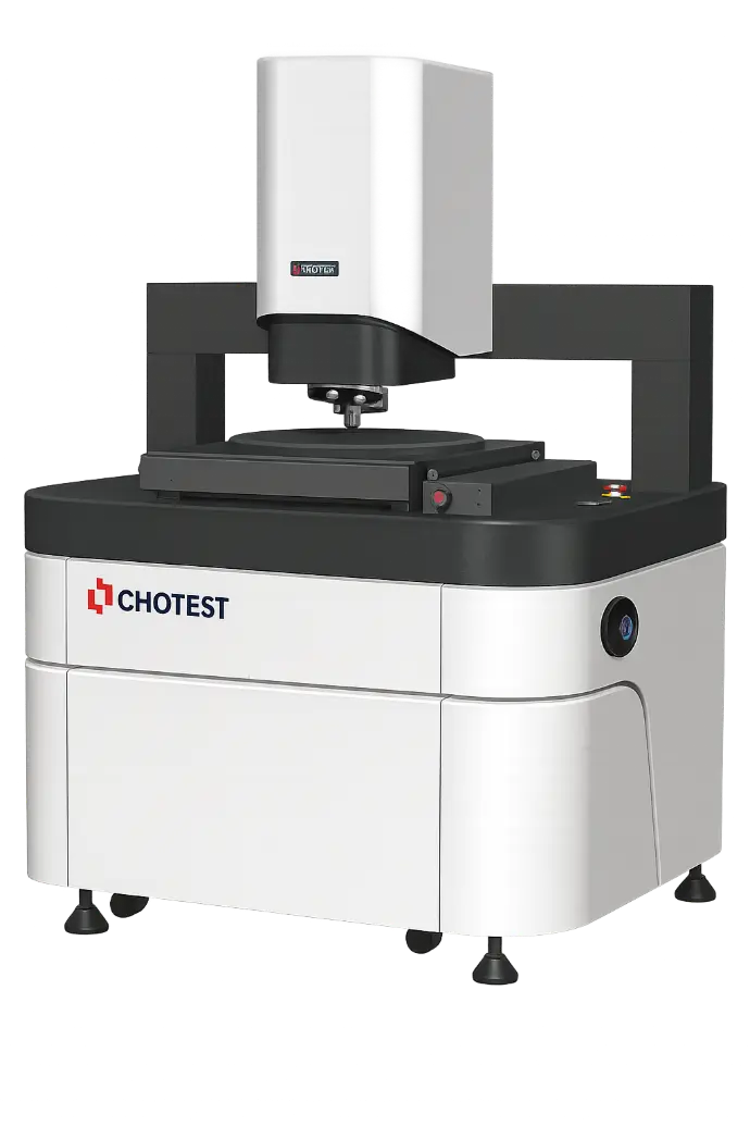
SuperView W3 – 3D Optical Surface Profilometer
White Light Interferometry | Nano 3D Surface Form & Roughness
Large-scale microscopic 3D form and roughness
The CHOTEST SuperView W3 is a state-of-the-art optical surface profiler designed for high-precision 3D surface analysis at the nanometric level. Using white light interferometry, it provides accurate, repeatable, and non-contact measurements of surface form, roughness, and step height — ideal for R&D and quality control in semiconductor, optics, micro-electronics, and materials industries.
Key Features
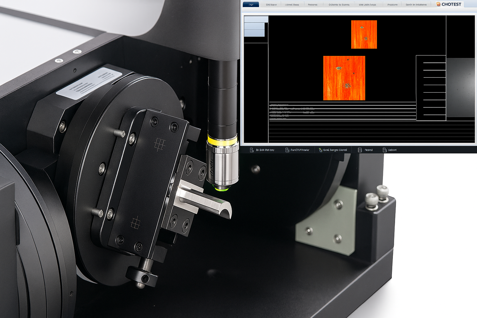
Dedicated Functions for Semiconductor Field
Measure prof
Measure film step-height of wafer ranging from 1nm~1mm.
Measure roughness of silicon cut sheet after grinding process, and can measure
dozens of small areas to obtain the average value by one click.
Support 6", 8" and 12" wafer measurement, and easy switch between 3 sizes of vacuum chucks by one click automatically.
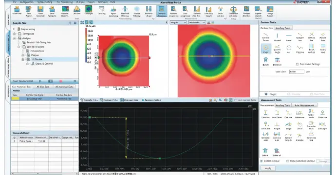
Software: XtremeVision 3D
The integrated XtremeVision 3D software combines:
3D image scanning & analysis
Automated measurement
Intelligent noise filtering
Hybrid scanning (white light interferometry + confocal)
It allows automatic feature recognition and step height measurement with repeatability as fine as 0.005μm and step accuracy of 0.08%.
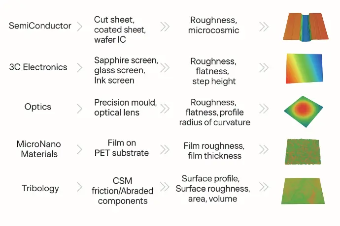
Application
micro-nano materials, micro-electro-mechanical system.
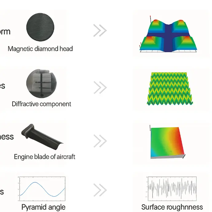
Application Cases
Measurement and analysis for various products, components and materials`surface form and profile characteristics, such as flatness, roughness, waviness, appearance, surface defect, abrasion, corrosion, gap,hole, stage, curvature, deformation, etc.
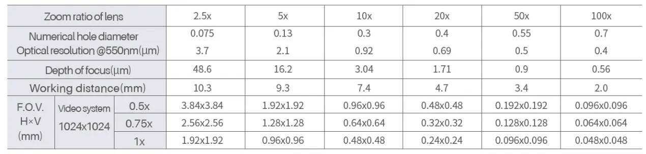
Lens Specification
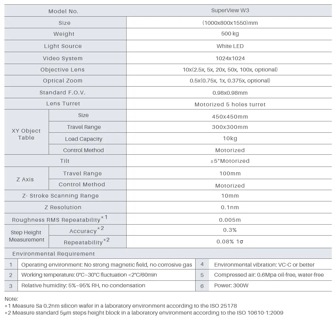
3D Optical Surface Profilometer SuperView W3
Large-scale microscopic 3D form and shape:
■ Large table ■ Applicable for 12" wafer ■ One-key automatic measurement Dedicated Functions for Semiconductor Field: • Measure profile trenches after laser grooving in the dicing process. • Measure film step-height of wafer ranging from 1nm~1mm. • Measure roughness of silicon cut sheet after grinding process, and can measure dozens of small areas to obtain the average value by one click. • Support 6", 8" and 12" wafer measurement, and easy switch between 3 sizes of vacuum chucks by one click automatically.